Overview
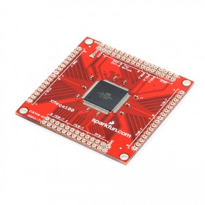
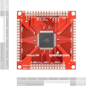
This is a breakout board for the 100-pin TQFP package of Atmel's ATxmega128A1. The ATxmega128A1 is a low power, high performance and peripheral rich CMOS 8/16-bit microcontroller based on the AVR enhanced RISC architecture.
Among the chip's many features are 128kB of flash memory, 8 kB SRAM, 78 I/O pins, eight 16-bit timers, sixteen 12-bit ADCs, four 12-bit DACs, eight USART, four SPI and four TWI interfaces. This powerful chip can process up to 32 MIPS when running at its maximum clock speed of 32MHz. The operating voltage of the xmega is 1.6 to 3.6VDC.
All VCC pins of the ATxmega128A1 are connected together and brought out to a single header pin, same goes for the GND and AVCC pins of the chip. We've also included decoupling capacitors, and a red power indicator LED; but beyond those we've tried to keep the board as simple and straightforward as possible. If you want to start developing with this chip, but don't want to deal with soldering it, this is the board for you!
Note: The 6 pins labeled ICSP are used to program the board through the PDI interface using the common 6 pin ICSP cable found on most AVR programmers. Also, this board ships with the example code shown below and the JTAGEN bit set to 1 (JTAG disabled, PDI enabled).
Fitur
- All pins of the ATxmega128A1 broken out to 0.1" spaced pins
- 0.1uF decoupling capacitors placed near VCC inputs of the chip
- 2x3 AVR ICSP connector broken out
- Red power indicator LED
- ATxmega128A1 Features:
- High-performance, low-power 8/16-bit microcontroller
- 1.6 - 3.6 VDC operating voltage
- 128 KBytes Flash
- 8 KBytes boot code
- 2 KBytes EEPROM
- 8 KBytes SRAM
- 4 DMA channels
- 32 MHz maximum clock frequency
- 78 programmable I/O pins
- Eight 16-bit timers
- Eight USARTs, four SPI, and four TWI interfaces
- Two Eight-channel (16), 12-bit, 2 Msps Analog to Digital Converters
- Two Two-channel (8), 12-bit, 1 Msps Digital to Analog Converters
Dimensi
- 55.88 x 55.88mm
Link Dokumentasi
- Schematic
-
Atmel's ATxmega128A1 Product Card
- Example C code (zip)


